
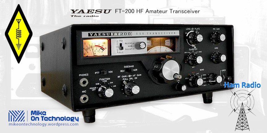
My Yaesu FT-200 HF band amateur transceiver review includes, instruction manuals, and video presentation of the transceiver.
Yaesu FT-200 Amateur Band HF Transceiver
The Yeasu FT-200 transceiver covers the amateur bands 80 through 10 metres. The transceiver provides transmission and reception of SSB (both USB and LSB are selectable), CW and AM. The transmitter provides ±240 W (two-tone) which is eqaul to approximately 300 PEP speech input.
Stability is achieved with a well designed VFO along with a 9 MHz IF crystal filter for good voice quality.
Features of the Yaesu FT-200 include VOX (voice operated changeover), a 100 kHz xtal controlled calibrator, ±5 Khz receiver offset tuning (clarifier). As well as these features, this transceiver is made to connect easily to the Yaesu FLDX-2000 Linear Amplifier.

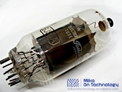
The Yaesu FT-200 transceiver is mainly a vacuum tube design, however several solid state transistors and diodes are also used. Yaesu made the right choice in sticking with vacuum tubes. At the time semiconductors were in the early years of development while vacuum tubes are well known for their wide dynamic range..
By using tubes the FT-200 receiver has a wide dynamic range, far superior than contemporary solid state receivers. Of course semiconductors have caught up, so now we can obtain suitable transistors with wider dynamic ranges.
Looking Inside the Yaesu FT-200
The photos below show the insides of the Yaesu FT-200 transceiver from several viewpoints.

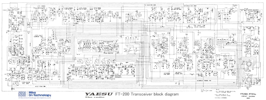
Yaesu FT-200 Circuit Description
As can be seen from the block diagram below, many of the transceiver sections are common to both the transmitter and receiver. We’ll examine the various stages, starting with the receiver. Then we look at the oscillator circuits.

Starting with the Receiver
After passing through the antenna Tx/Rx relay the signal from the antenna through the antenna tuning circuit before being fed to the grid of RF amplifier tube V2 (a 6BZ6) which amplifies the signal. This is passed through the following tuned circuit, then to the receive mixer tube V1 (a 6U8) pentode grid.
The local oscillator output is fed to the cathode of this mixer stage and the IF is taken from the mixer plate. The IF signal passes through the 9 MHz xtal filter after which it goes to a 2 stage amplifier consisting of V104 (6BA6 and V103 (6BZ6). This then goes to the power grid of the detector V102A (½ 12AX7) which operates as a as a product detector.
With the BFO signal applied to it’s cathode, when receiving CW and SSB signals V102B (½ 12AX7) works as an anode detection type amplifier for AGC control. With no signal applied plate current is zero, while with signal the plate current develops. This results in a negative plate voltage which is applied via diode D103 to the AGC line.
The AGC (Automatic gain control) circuit provides the desired AGC characteristics which are fast attack and slow decay for SSB and CW. The internal resistance of D103 is low in forward voltage conditions, while it is high under reverse voltage conditions. The AGC voltage is applied to the RF and IF stages which results in the circuit’s ability to handle a wide range of signal levels.
The output from the detector stage is fed to the 2 diodes D101 and D102, ANL, then via the AF gain control through the 6BM8 audio amplifier output tube. The audio output then goes to a speaker.
Transmitter Stage
SSB, AM and CW Signal Generation
The carrier oscillator tube V106 (12AU7) generates a signal that is sent to the 1st grid of tube V107 (7360) balanced modulator. The audio signal from the microphone amplifier is taken to the modulating grid of the balanced modulator. A suppressed carrier DSB (double sideband) signal is produced at the balanced modulator plate. The DSB signal is passed through the crystal filter XF101. One sideband is removed hance a 9 MHz SSB signal results at the filter output.
To produce AM, which in the case with the Yaesu FT-200 is sideband plus inserted carrier, the balanced modulator is unbalanced by the mode switching circuitry which then allows the carrier to pass through. At the same time the carrier frequency is shifted by a varicap diode so that the carrier passes freely through the filter passband. The amount of carrier insertion is adjustable by the AM carrier control VR8.
To transmit in CW mode the audio from the microphone amp is disabled. Similar to AM mode the modulator is again unbalanced to allow the full carrier to pass through.
A1.5 kHz signal is generated by the audio tone oscillator TR5033. This is applied to the balanced modulator in order to provide a tuning signal at the filter centre frequency. The level of this signal is controlled by the microphone gain control.
IF, Signal Mixing and Amplifier Stages
The 9 MHz signal passes through the filter. The signal then is amplified by IF amplifier V104 (6BA6) and sent to the grid of the mixer tube V4 (6EJ7) along with the local oscillator signal. The resulting difference between these two signals appears at the plate tuned circuit of the mixer which is then the output signal frequency. (On 14 MHz additive mixing is used.)
This signal is amplified by the tuned driver circuit V5 (12BY7) before going to the power amplifier stage. The power amplifier consists of a pair of 6JS6A sweep tubes V6 & V7 which operate in class AB2 for maximum power output.
Other Transmitter Circuitry
When the AC component of the PA grid current is overdriven by peak signals diodes D4 and D5 to provide an ALC (Automatic level control) voltage to the IF amplifier stage, thereby reducing the gain and helps maintain low distortion levels.
The power amplifier plate circuit attenuates higher order harmonics while also allowing easy matching of output impedance to antenna feedline impedance.
On phone both PTT (Push to talk) and VOX (VOice operated changeover) is available. In VOX mode a signal sample from the microphone is applied at the grid of V8. This then goes to V9A, is rectified by diode D2 (SH-1) thereby producing a positive bias on the grid of the relay tube V9B. This cause plate current to rise thereby operating the relay.
On CW there are 2 keying methods, straight or “break-in”. Break-in is produced by keying the audio oscillator tone applied to the VOX amp as well as transmitter bias on V107, V4, V5,V6 and V7. The tone signal can be heard from the speaker while keying thereby providing sidetone monitoring.
Yaesu FT-200 Oscillator Circuits
The Yaesu FT-200 crystal oscillators generate the carrier and the band switched heterodyne oscillator. The VFO is a self-controlled oscillator which operates at a frequency low enough to ensure good stability. Other oscillators produce the 100 KHz xtal calibration signal and the AF tone. There’s also an optional xtal oscillator for fixed channel operation.
Carrier Oscillator
The carrier oscillator is crystal controlled. The circuit uses a 12AU7 double triode with xtals of 8.9985 MHz and 9.0015 MHz. With the 8.9985 MHz xtal it is operative on the 7 and 14 MHz bands. When the 9.0015 MHz xtal is in use it is operative on the 3.5, 21 and 28 MHZ bands. When the the selector switch is placed in the reverse position the crystal oscillator sections are changed.
The carrier oscillator also functions as a BFO in receive mode. On AM & CW the 9.0015 MHz xtal is used, however it’s frequency is lowered by 200 Hz by the diode switch D104 (1S1007) thereby bringing the carrier into the filter passband.
Bandswitched Heterodyne Oscillator
A 2SC372 transistor forms the heterodyne oscillator and operates on the 7, 21 and 28 MHz bands. A xtal for 28.000 to 28.500 comes with the transceiver. However the rest of the 28.5 to 30 MHz band requires 3 more optional xtals for full coverage.
VFO Self-oscillator
The VFO is a transistor Colpitts oscillator circuit using a 2SC372 transistor while another 2SC372 transistor forms a buffer. The VFO features linear tuning over the range 5 MHz to 5.5 MHz. The passband filter at the output allows tuning the circuit to pass the 5 MHz to 5.5 MHz range.
A varicap diode D401 (1S145) provides the clarifier control ±5 kHz when receiving.
Crystal Calibrator
The calibrator is a crystal controlled oscillator using a 2SC367 transistor with a 100 kHz xtal. A 1S1007 diode forms a harmonic generator thereby providing check points every 100 kHz on the tuning dial.
AF Oscillator
The AF oscillator is a phase shift circuit generating a pure audio tone signal at 1.5 kHz to supply the transmitter tune-up signal as well as allowing CW sidetone monitoring.
Local Oscillator Mixer Circuit
The VFO output is applied to grid 1 of the V3 (6CB6) mixer, while the heredyne oscillator output to the cathode of this tube. The resulting beat frequency is selected by the plate tuned circuit.
Meter Circuit
Meter M1 has a 1 mA full scale movement. The meter is connected to the 2nd IF stage. It reads changes in the cathode voltage of V103 resulting from variations in the AGC voltage to indicate receiver “S” units.
In use the meter is automatically switched by a relay RL101 indicating relative power output. power amplifier cathode current and ALC voltage. The meter scale is fully calibrated and the transmitter metering functions are selected by the front panel mounted slide switch.
Voltage Regulator Circuit
The voltage regulator is built on a printed circuit board (PCB) and provides 9V DC for all the transistor oscillators. 2 transistors a 2SC372 and a 2SC376 are used together with 2 zener diodes 1S331 and 1S336. Voltage levels can be set by adjusting the variable resistor VR501.
Yaesu FT-200 Circuit Diagram
SPECIFICATIONS
| GENERAL | |||
| Type: | Amateur HF transceiver | ||
| Frequency range: | 10-80 m in 8 bands 3.5-4.0 MHz 7.0-7.5 MHz 14.0-14.5 MHz 21.0-21.5 MHz 28.0-28.5 MHz 28.5-29.0 MHz 29.0-29.5 MHz 29.5-30.0 MHz |
||
| Tuning steps: | Continuous | ||
| Mode: | A3J SSB (USB / LSB), A3H AM, A1 (CW) | ||
| Frequency stability: | 100 Hz / 30 minutes (After warm up) | ||
| Antenna impedance/connector: | 50-75 ohms / SO-239 | ||
| Tubes and semiconductors: | 16 tubes, 15 diodes, 7 transistors | ||
| Operating Voltage / Frequency | 110 to 240 VAC (separate FP-200 PSU) / 50 – 60 Hz | ||
| Dimensions (W*H*D): | 335 mm wide x 140 mm high x 280 mm deep | ||
| Weight: | 10 Kg | ||
| RECEIVER SECTION | |||
| Receiver system: | Single conversion superheterodyne IF: 9 MHz |
||
| Sensitivity: | 0.5 uV (10 dB S/N) | ||
| Selectivity: | SSB: 2.3 KHz (-6 dB), 4 KHz (-60 dB) | ||
| Image rejection ratio: | 50 dB | ||
| IF interference ratio: | 50 dB | ||
| AF output power: | 1 W at 10% distortion | ||
| Audio output impedance: | 8 Ω and 600 Ω | ||
| TRANSMITTER SECTION | |||
| RF output power: | SSB: Max 100 W | ||
| 3rd order intermodulation products: | -30 dB (P.E.P.) | ||
| Carrier suppression: | -40 dB | ||
| Sideband suppression: | -50 dB @ 1kHz | ||
| MISCELLANEOUS | |||
| Manufactured: | Japan, 1969-197x (Discontinued) | ||
| Additional info: | 2 x 6JS6A finals Early version had a silver front, while later version was black with slightly changed functions. Also sold as Henry Tempo One and Sommerkamp FT-250. |
||
| Related documents: | |||
| Options/Accessories: |
|
VIDEOS
Current Availability
I found several FT-200 transceivers for sale on EBay. Prices range from around $190.00 (R2860.00 ZAR in 2022) to $250.00 (R3370.00 ZAR in 2022)
The output amplifier tubes (which claim to be new) could also be found online for about $35 (R530.00 ZAR in 2022) each.
These are not bad prices. The FT-200 prices seen definitely make this rig a good option for radio amateurs today.
